

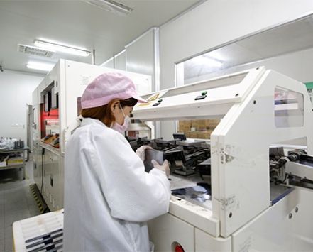
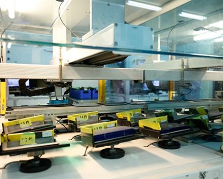
inspection
Purpose: Eliminate abnormal silicon wafers to ensure product quality.
Electrical testing: resistivity; thickness / TTV; conductivity type; minority life.
Optical inspection: size; verticality; chipping; surface stains; cracks; holes
With advanced raw material silicon purification technology:ENERGY can use patented technology to purify metallurgical silicon to produce solar cells. The cost of upgraded silicon wafers fully purified by this technology is much lower than the original electronic grade silicon wafers, thus reducing the cost of high quality silicon solar cells;
Specializing in the production of high conversion rate crystalline silicon photovoltaic cells:Silicon-based cell sheets developed through various technological innovations have extremely high conversion efficiency, thereby reducing the cost of mass production;
Large-scale photovoltaic module production technology based on second-generation battery chips:Working closely with equipment manufacturers to enable JA Solar to produce unique thin film-based solar cells and components on a lower cost basis;
Committed to the long-term research of more advanced third-generation photovoltaic technology:Our position is to reduce costs while maintaining the economic and environmental cost advantages of thin film and nanostructure technology through significant improvements in conversion efficiency.
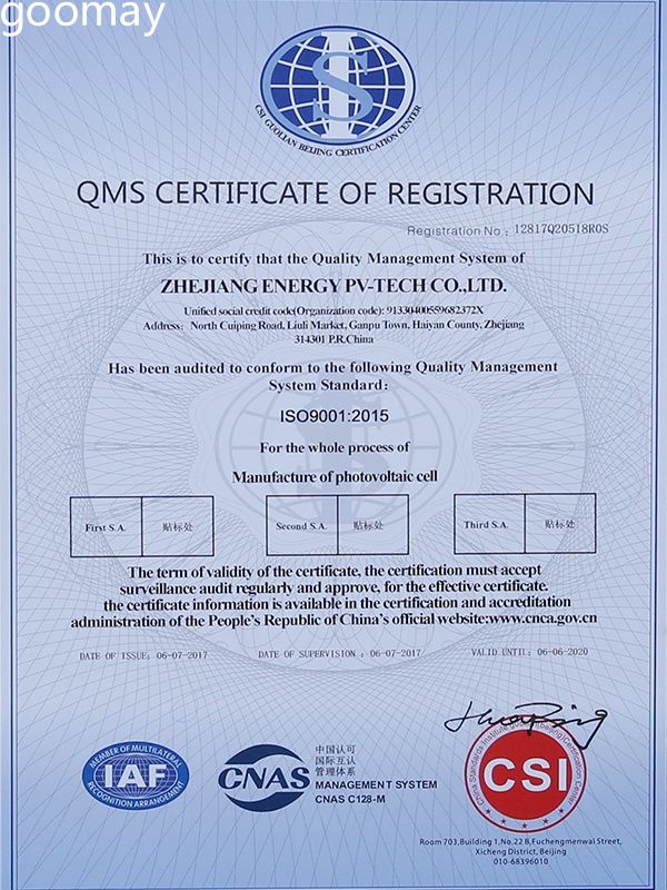
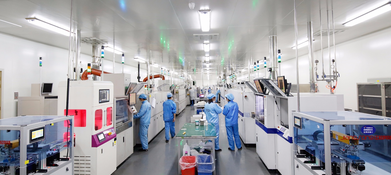
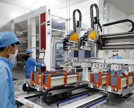
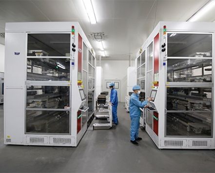
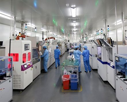
ENERGY is convinced that “product quality is the starting point for value and dignity”, and that a scientific quality management system will be established at the initial stage, and “continuous improvement” will become an inseparable part of the company culture. Ai Neng Ju Photovoltaic's leading design capability, first-class production and professional testing equipment, fine production management, strict quality management system, excellent staff training system and employee incentive mechanism are all important guarantees for high quality and reliable products.
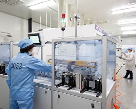
Purpose: Eliminate abnormal silicon wafers to ensure product quality.
Electrical testing: resistivity; thickness / TTV; conductivity type; minority life.
Optical inspection: size; verticality; chipping; surface stains; cracks; holes
Purpose: To increase the absorption of light on the surface of the solar cell sheet and reduce reflection.
The method is realized: the high-concentration acid solution is used to corrode the surface of the silicon wafer to remove the mechanical damage layer, and the suede surface of the egg-like depression is formed to increase the absorption of sunlight and reduce the reflectivity.
Objective: To prepare a PN junction.
Implementation method: by high temperature diffusion, an N layer is diffused on the surface of the P-type silicon wafer to form a PN junction.
Purpose: To remove the PN junction at the edge of the wafer to prevent short circuits and to remove the phosphosilicate glass (PSG) formed after diffusion.
The method comprises the steps of: floating the silicon wafer above the chemical agent, oxidizing the elemental silicon on the surface by the strong oxidative oxidation of nitric acid, and then reacting with the hydrofluoric acid to form silicon fluoride dissolved in water, thereby achieving the purpose of removing the edge of the silicon wafer. .
OBJECTIVE: A thin layer with a refractive index lower than that of the silicon wafer itself is deposited on the surface of the diffused silicon wafer to reduce surface reflection when light is incident on the silicon wafer. Therefore, the thin layer is called an anti-reflection film.
Implementation method: a plasma-enhanced chemical vapor deposition technique is used to deposit a silicon nitride anti-reflection film on the surface of the cell sheet, and hydrogenation is also performed at the same time of film formation, so that the solar cell is enhanced while enhancing the absorption of light. Good surface and in vivo passivation while increasing short circuit current and open circuit voltage.
Objective: To prepare electrodes and aluminum back field on the front and back sides of the silicon wafer.
Implementation method: Using screen printing technology, the corresponding graphics are printed on the front and back sides of the silicon wafer with silver paste and aluminum paste.
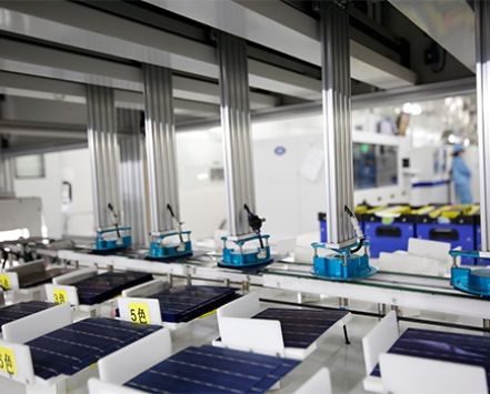
Purpose: The solar cell produced is binned according to the performance result (conversion efficiency).
Implementation method: test the performance parameters of the solar cell by simulating the sun light to the surface of the cell sheet.
Purpose: To eliminate the appearance of defective products, to classify the color of the same efficiency gear cell.